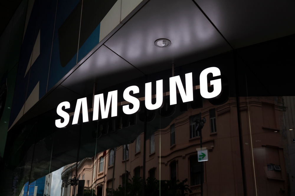
Samsung has secured a landmark $6.4 billion in funding from the CHIPS and Science Act, fueling its ambitious plans to establish a comprehensive chipmaking hub in Texas. This investment, exceeding $40 billion, will see the creation of new foundries, R&D facilities, and advanced packaging capabilities – a major win for the US semiconductor industry.
As reported by DigiTimes, the funding highlights the government’s push to revitalise domestic chip production. Samsung’s investment promises thousands of jobs and positions Texas as a vital center for cutting-edge technologies, including 4nm and 2nm process nodes.
Crucially, Samsung’s expansion will encompass advanced packaging technologies like HBM and 2.5D in high demand for AI and high-performance computing. This comprehensive approach underscores Samsung’s commitment to becoming a key player in the global semiconductor landscape.
Beyond its facilities, Samsung is actively cultivating a local supplier ecosystem. This strategic move strengthens the region’s supply chain and bolsters its attractiveness as a hub for electronics innovation. The Samsung-led transformation promises to benefit not only the company but the entire US semiconductor sector for years to come.
Thousands of senior engineers and procurement professionals subscribe to our LinkedIn Market Intel newsletter – get yours here
For more help with looking at supply chain options, contact Astute Electronics